
 MENU
MENU 

The Lurie Nanofabrication Facility gets a new director
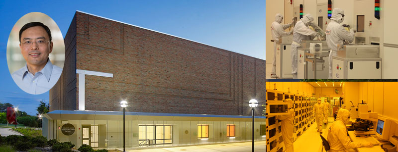
Prof. Wei Lu has been named the new director of the Lurie Nanofabrication Facility (LNF), effective September 1, 2016.
 Enlarge
Prof. Wei Lu has been named the new director of the Lurie Nanofabrication Facility (LNF), effective September 1, 2016. The LNF is a world class cleanroom facility, open to the public, with over 13,500 sq. ft. of state-of-the-art cleanroom space that provides researchers the ability to fabricate a sweeping array of solid-state materials, devices, circuits, and microsystems using silicon, compound semiconductors, organic, and other emerging materials.
Research conducted in the LNF has led to improved neural probes for treatment of Parkinson’s and other diseases; novel methods to uncover the mysteries of the brain; integrated sensors for use in stents for the carotid arteries; nanoscale lasers; cochlear implants; transparent and flexible electronics; high-efficiency lighting; integrated microsystems for autonomous data gathering; colorful and artistic solar cells; new devices for weapons detection and medical imaging; carbon nanotube coating for cloaking; and much more.
As the single largest user of the facility, Prof. Lu conducts research in emerging electrical devices such as resistive random-access memory (RRAM), neuromorphic circuits, and nanowire transistors. His research has resulted in the successful startup company, Crossbar, Inc., which is now delivering commercial memory products to customers.
“I couldn’t do much without the LNF, except for simulations,” said Lu. “All of my research projects depend critically on this facility.”
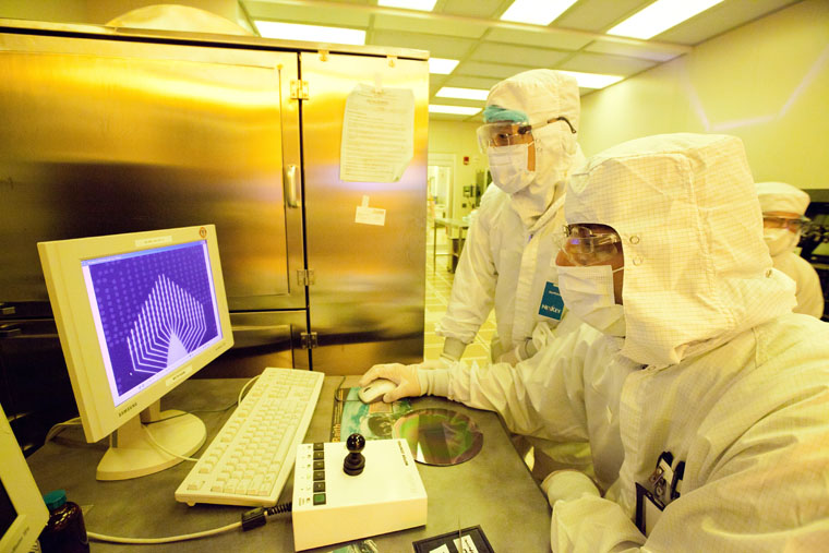 Enlarge
Prof. Lu works with circuit groups and computer scientists from Michigan and across the U.S. to develop energy-efficient computing hardware based on technologies developed at the LNF. To achieve better device and circuit performance he is developing engineered materials that do not exist in nature. He collaborates with materials scientists (Prof. Emmanouil Kioupakis and Prof. Pierre Poudeu-Poudeu) to design these materials from the ground up at the atomic level.
Prof. Lu says that the scale of the LNF combined with its variety of tools make it unique among academic nanofabrication facilities. “Most any major capability one can think of, we have it here. The LNF offers extensive expertise and equipment that cover most every aspect of semiconductor research, from materials growth and individual process developments to systems level integration. We integrate different heterogeneous components to form a functional system that is more powerful than any single device in the system.”
 Enlarge
Working with the Lab Manager, Dr. Sandrine Martin, other LNF staff, faculty users across the College of Engineering, as well as students and external users, Prof. Lu plans to maintain the excellent service currently provided to users of the facility.
Beyond that, “A key role of mine,” said Lu, “is to expand our capabilities with future research directions in mind.”
The Lab Today
 Enlarge
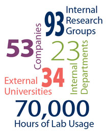
In recent years, more than 470 individuals made use of the LNF. Most were U-M researchers from many different engineering disciplines as well as the Cancer Center, Pediatrics, Psychology, Computation, Medicine & Bioinformatics, and more. The remaining users came from local startup companies, larger corporations, government agencies, and 25 universities (including institutions in Mexico, Canada, and Turkey).
Among the grand challenges LNF research addresses through specific technology are: wireless implantable microsystems to address a wide variety of medical challenges, including glaucoma, epilepsy, deafness, cardiovascular disease, and diabetes; microelectrode arrays for reverse-engineering the brain; biomimetic microsystems for intelligent electronic systems; diagnostic biomedical microsystems for detection of cancer, TB, and DNA; high-efficiency energy converters and power electronics; environmental monitoring systems; infrastructure monitoring; and sensors for personal and national security.
It hosts one of the leading research centers worldwide on MEMS and microsystems, with applications for integrated sensors/actuators, microsystems, biology, medical microsystems, chemistry, and environmental monitoring.
The LNF has established technologies for bulk and surface micromachining, MEMS fabrication, and MEMS-CMOS integration. Equipment is available for thin film deposition and growth, optical and e-beam lithography, nanoimprinting, wet and dry etching, electrochemical deposition, chemical mechanical planarization, wafer bonding, wafer dicing, wire bonding, metrology, and more.
The LNF also provides expertise in environmental and geological sciences, including sensors for underwater observatories, and in computation and modeling of MEMS and microfluidic devices and structures.
 Enlarge
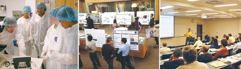
In addition to pure research, the LNF offers a broad range of expertise and equipment to support high impact education, research and business development activities. The LNF team offers professional workshops to the community and outreach events to the general public. They also hold an annual LNF Users Symposium with technical talks, poster sessions, and the opportunity for valuable networking.
A History of Micro and Nano in the Lab
Since its earliest beginnings, users of the lab have been breaking new ground, while the lab directors worked tirelessly to make sure the lab facility itself kept pace with technology.
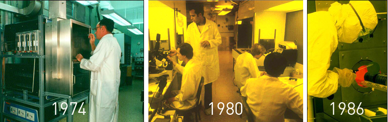
The LNF has its roots in the Electron Tube Lab, established in 1946 by William Gould Dow. Its primary focus was high-power microwave and millimeter-wave tube technology. The lab was renamed the Electron Physics Laboratory in 1958, reflecting research that had expanded to include semiconductors.
In the early 1970’s, the Lab was remodeled to expand its fabrication capabilities, enabling the first program at Michigan in integrated sensors and circuits. About a decade later, following the addition of key equipment, the Lab was renamed the Solid-State Electronics Laboratory (SSEL) in 1984. Though primitive by today’s standards, it was sufficient to establish Michigan as an early leader in the emerging field of micro-electro-mechanical-systems (MEMS), but not for long. The future was in sight, but the current lab was now insufficient for Michigan to participate in it for long.
 Enlarge
With the help of some key players, including the State of Michigan, a new lab facility was constructed on North Campus in 1986 as part of the newly constructed EECS Building. With this dramatic upgrade to the existing facility, Michigan research expanded into a wide variety of micro devices including neural probes, cochlear implants, gas sensors, pressure sensors, imagers, photonics, and nano devices.
By the early 2000s, the equipment in the Solid-State Fabrication Facility was over 15 years old. Replacement parts were no longer available for many tools, and it was again clear that to remain competitive, a major expansion of the facility was essential. Thanks largely to alumni and other donors, the lab was once again greatly expanded and then outfitted with about $70M in infrastructure and equipment upgrades.
The newly-named Lurie Nanofabrication Facility, named after primary benefactor Anne Lurie, was completed in 2008. It became a nationwide user facility, thanks in large part to its membership in the NSF National Nanotechnology Infrastructure Network (NNIN), which ended in 2015.
Prof. Lu, the twelfth director of the lab, takes over from Prof. Euisik Yoon, director of the International Program for the Advancement of Neurotechnology and accompanying International Conference for Advanced Neurotechnology.
LNF Users Symposium: December 1, 2016
The Lurie Nanofabrication Facility at the University of Michigan
The Lurie Nanofabrication Facility is a state-of-the-art cleanroom at the University of Michigan that enables researchers to work with many different types of materials. The lab is open to users from both the university and industry, and has helped make some of the hottest nanotechnology possible.
Here’s some of the research conducted by the 93 U-M researcher groups who use the LNF:
 Enlarge
 Enlarge
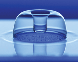 Enlarge
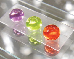 Enlarge
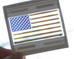 Enlarge
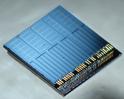 Enlarge